
Finding the Hidden Field Sources
in Switching Converters
High dv/dt Areas, High di/dt Loops, and Geometry Behind Converter Noise & Failures
Applied Engineering Insight
Engineering Fundamentals
Issue 01 / June 2026 · Martin Weiss
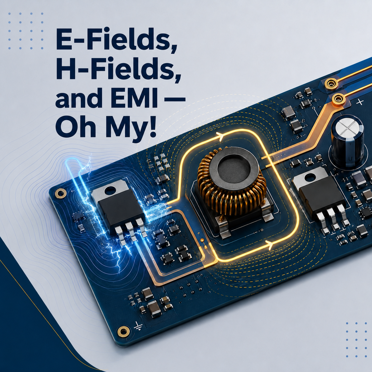
A converter schematic can be correct while the physical implementation is already creating its own failure path. This Applied Engineering Insight shows how to identify high-dv/dt areas, high-di/dt loops, package structures, and return paths before they become EMI, ringing, overshoot, or device-stress problems.
Schematic shows intent.
Layout defines field behavior.
More Topics
Test Systems & Validation
Data Integrity & Measurement
Engineering Safety
References cited in this Insight (with permission of owners):
1) Data estimate derived from: “Does the Assembly Orientation of an SMPS Inductor Affect Emissions?”
Analog Dialogue, Analog Devices, Vol. 55, No. 2, June 2021.
2) PCB Layout for Switchmode Converters: The Loops That Determine Whether Your Design Works
Philip Bassett, June 2026, https://switchmode.io/
Additional resource related to SiC devices:
1) Mitigating EMI with SiC Solutions in Renewable Energy and Grid-Connected Power Converters, Wolfspeed, PRD-08907